Guidelines for OpenCL BSP Floorplanning
- Begin with flat compilation to understand where all main components of the BSP gets placed naturally (especially the IP blocks with I/O connections such as PCIe® or DDR). While designing the BSP, you might have to consider establishing pipeline stages in between the IPs to close timing. You should first run a flat compile seed sweep to identify the recurrent failing paths, and then attempt to fix them.
Tip:
- A good timing closure rate over flat compile seed sweeps will have higher chances of closing base compile timing.
- If you observe consistent failures in mm_interconnect* (component added by Qsys), then open the System with Qsys Interconnect viewer and observe the complexity of the failing interconnect. You can add pipelining flipflops in the viewer to improve timing. If you still cannot address the issue, you might have to break down the mm_interconnect* critical path by adding Avalon® pipeline bridges.
- During base compilation, start with LogicLock® on kernel region that contains freeze_wrapper_inst|kernel_system_inst. With no other restrictions, Intel Quartus® Prime can place the BSP hardware freely in the remaining static region of the chip. Use the flat compile and chip planner to identify the size and location of the BSP hardware, such as PCIe® and DDR. Then, reserve the kernel region by using LogicLock® while avoiding the main clustered areas of the BSP hardware.
Tip: If the chip family used is same as the reference platform and if the BSP components are similar, it might be faster to start with the LogicLock® regions for freeze_wrapper_inst|kernel_system_inst that is shipped with the OpenCL reference BSP and work through the failures.
- You might add the following additional components to your BSP:
- Memory banks: If you add more memory banks, you should identify the I/O bank location since you may need to add pipeline bridges to meet timing.
- I/O channels: You can add I/O channels such as video, Ethernet, or serial interface. If you add I/O channels, you should identify the I/O bank location since you might need to apply new LogicLock® regions for pipelining if closing timing is difficult.
Tip: If you need to add pipeline bridges (for example, due to large routing delays causing timing failures), then consider the routing distance from source to destination logic in the chip and release some space reserved for the kernel region. - Follow these general guidelines when reserving LogicLock® regions for the kernel:
- Attempt to place all DSP columns in the kernel_system unless required by the BSP.
- Attempt to reserve more resources for the kernel_system.
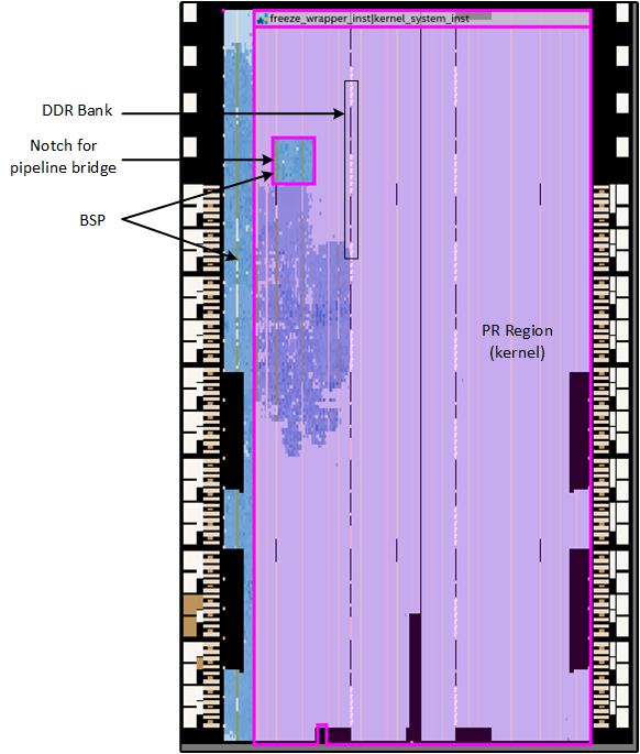
- Attempt to keep the number of notches in the kernel region to a minimum. The following figure illustrates a notch that was added to place a pipeline bridge between PCIe® and DDR bank.
Figure 1. OpenCL BSP Floorplan for Intel Arria® 10 GX in the 17.0 Release