Visible to Intel only — GUID: jex1538582571209
Ixiasoft
Product Discontinuance Notification
1. Introduction
2. First Time Designer's Guide
3. Hardware System Design with Intel® Quartus® Prime and Platform Designer
4. Software System Design with a Nios® II Processor
5. Nios® II Configuration and Booting Solutions
6. Nios® II Debug, Verification, and Simulation
7. Optimizing Nios® II Based Systems and Software
3.1. FPGA Hardware Design
3.2. System Design with Platform Designer
3.3. Interfacing an External Processor to an Intel FPGA
3.4. Avalon-MM Byte Ordering
3.5. Memory System Design
3.6. Nios® II Hardware Development Tutorial
3.7. Platform Designer System Design Tutorial
3.8. Hardware System Design with Intel® Quartus® Prime and Platform Designer Revision History
3.6.4.1. Analyzing System Requirements
3.6.4.2. Defining and Generating the System in Platform Designer
3.6.4.3. Integrating the Platform Designer System into the Intel® Quartus® Prime Project
3.6.4.4. Developing Software with the Nios® II Software Build Tools for Eclipse
3.6.4.5. Running and Debugging Software on the Target Board
3.6.4.6. Varying the Development Flow
3.6.5.1. Install the Design Files
3.6.5.2. Analyze System Requirements
3.6.5.3. Start the Intel® Quartus® Prime Software and Open the Example Project
3.6.5.4. Create a New Platform Designer System
3.6.5.5. Define the System in Platform Designer
3.6.5.6. Integrate the Platform Designer System into the Intel® Quartus® Prime Project
3.6.5.7. Download the Hardware Design to the Target FPGA
3.6.5.8. Develop Software Using the Nios® II SBT for Eclipse
3.6.5.9. Run the Program on Target Hardware
3.6.5.5.1. Specify Target FPGA and Clock Settings
3.6.5.5.2. Add the On-Chip Memory
3.6.5.5.3. Add the Nios® II Processor Core
3.6.5.5.4. Add the JTAG UART
3.6.5.5.5. Add the Interval Timer
3.6.5.5.6. Add the System ID Peripheral
3.6.5.5.7. Add the PIO
3.6.5.5.8. Specify Base Addresses and Interrupt Request Priorities
3.6.5.5.9. Generate the Platform Designer System
3.7.1. Software and Hardware Requirements
3.7.2. Download and Install the Tutorial Design Files
3.7.3. Open the Tutorial Project
3.7.4. Creating Platform Designer Systems
3.7.5. Assemble a Hierarchical System
3.7.6. Viewing the Memory Tester System in Platform Designer
3.7.7. Compiling and Downloading Software to a Development Board
3.7.8. Debugging Your Design
3.7.9. Verifying Hardware in System Console
3.7.10. Simulating Custom Components
3.7.11. View a Diagram of the Completed System
3.7.4.1.1. Create a New Platform Designer System and Set up the Clock Source
3.7.4.1.2. Add a Pipeline Bridge
3.7.4.1.3. Add a Custom Pattern Generator
3.7.4.1.4. Add a PRBS Pattern Generator
3.7.4.1.5. Add a Two-to-One Streaming Multiplexer
3.7.4.1.6. Verify the Memory Address Map
3.7.4.1.7. Connect the Reset Signals
3.7.4.1.8. Save the System
3.7.4.2.1. Create a New Platform Designer System and Set Up the Clock Source
3.7.4.2.2. Add a Pipeline Bridge
3.7.4.2.3. Add a Custom Pattern Checker
3.7.4.2.4. Add the PRBS Pattern Checker
3.7.4.2.5. Add a One-to-Two Streaming Demultiplexer
3.7.4.2.6. Verify the Memory Address Map
3.7.4.2.7. Connect the Reset Signals
3.7.4.2.8. Save the System
4.1.1. Intel Command-Line Tools for Board Bringup and Diagnostics
4.1.2. Intel Command-Line Tools for Flash Programming
4.1.3. Intel Command-Line Tools for Software Development and Debug
4.1.4. Intel Command-Line Nios® II Software Build Tools
4.1.5. Rebuilding Software from the Command Line
4.1.6. GNU Command-Line Tools
4.1.6.1. nios2-elf-addr2line
4.1.6.2. nios2-elf-gdb
4.1.6.3. nios2-elf-readelf
4.1.6.4. nios2-elf-ar
4.1.6.5. Linker
4.1.6.6. nios2-elf-size
4.1.6.7. nios2-elf-strings
4.1.6.8. nios2-elf-strip
4.1.6.9. nios2-elf-gdbtui
4.1.6.10. nios2-elf-gprof
4.1.6.11. nios2-elf-gcc and g++
4.1.6.12. nios2-elf-c++filt
4.1.6.13. nios2-elf-nm
4.1.6.14. nios2-elf-objcopy
4.1.6.15. nios2-elf-objdump
4.1.6.16. nios2-elf-ranlib
4.2.2.4.1. Software Example Designs
4.2.2.4.2. Selecting the Operating System (HAL versus MicroC/OS-II RTOS)
4.2.2.4.3. Configuring the BSP Project
4.2.2.4.4. Configuring the Application Project
4.2.2.4.5. Makefiles and the Nios® II Software Build Tools for Eclipse
4.2.2.4.6. Building and Running the Software in Nios® II Software Build Tools for Eclipse
4.4.4.1. Performance Counter Advantages
4.4.4.2. Timer Advantages
4.4.4.3. Performance Counter and Timer Hardware Considerations
4.4.4.4. Performance Counter and Timer Software Considerations
4.4.4.5. Performance Counter Software Considerations
4.4.4.6. The Global Counter
4.4.4.7. Hardware Considerations
4.4.4.8. Tutorial: Using Performance Counters and Timers
4.4.5.1. nios2-elf-gprof –annotated-source Switch Has No Effect
4.4.5.2. Writing to the Registers of a Nonexistent Section Counter
4.4.5.3. Output From a printf() or perf_print_formatted_output() Call Near the End
4.4.5.4. Fitting a Performance Counter in a Hardware Design That Consumes Most
4.4.5.5. The Histogram for the gmon.out File Is Missing, Even Though My main()
5.2.1. Introduction to Nios® II Booting Methods
5.2.2. Nios® II Processor Booting from On-Chip Flash (UFM)
5.2.3. Nios® II Processor Booting from EPCQ Flash
5.2.4. Nios® II Processor Booting from QSPI Flash
5.2.5. Nios® II Processor Booting from On-Chip Memory (OCRAM)
5.2.6. Nios® II Processor Booting from CFI Flash
5.2.7. Summary of Nios® II Processor Vector Configurations and BSP Settings
5.2.3.1. Intel FPGA Serial Flash Controller (EPCQ) Overview
5.2.3.2. Nios® II Processor Design, Configuration, and Boot Flow
5.2.3.3. Nios® II Processor Application Execute-In-Place from EPCQ Flash
5.2.3.4. Nios® II Processor Application Copied from EPCQ Flash to RAM Using Boot Copier
5.2.3.5. EPCQ HAL Driver
5.2.4.1. Nios® II Processor Design, Configuration and Boot Flow
5.2.4.2. Nios® II Processor Application Executes In-Place from General Purpose QSPI Flash ( Intel® MAX® 10)
5.2.4.3. Nios® II Processor Application Copied from General Purpose QSPI Flash to RAM Using Boot Copier ( Intel® MAX® 10)
5.2.4.4. Nios® II Processor Application Executes In-Place from Configuration QSPI Flash (Other FPGA devices)
5.2.4.5. Nios® II Processor Application Copied from Configuration QSPI Flash to RAM Using Boot Copier (Other FPGA devices)
5.3.1. Assumptions About the Reader
5.3.2. Implementing a Custom Boot Copier
5.3.3. Default Nios® II Boot Copier
5.3.4. Advanced Boot Copier Example
5.3.5. Implementing the Advanced Boot Copier Example
5.3.6. Small Boot Copier Example
5.3.7. Implementing the Small Boot Copier Example
5.3.8. Debugging Boot Copiers
5.3.9. Externally Controlling the Nios® II Boot Process
5.3.5.1. Setting Up the Software Tools and Development Board
5.3.5.2. Creating a Suitable Hardware Design
5.3.5.3. Building the Advanced Boot Copier
5.3.5.4. Building a Test Application to Boot
5.3.5.5. Packing the Test Application in a Boot Record
5.3.5.6. Booting Directly From CFI Flash Memory
5.3.5.7. Booting CFI or EPCS/EPCQ Flash From On-Chip Memory
5.3.5.8. Running the Advanced Boot Copier Example
6.2.1.1.1. Nios® II System ID
6.2.1.1.2. Project Templates
6.2.1.1.3. Configuration Options
6.2.1.1.4. Nios® II GDB Console and GDB Commands
6.2.1.1.5. Nios® II Console View and stdio Library Functions
6.2.1.1.6. Importing Projects Created Using the Nios® II Software Build Tools
6.2.1.1.7. Selecting a Processor Instance in a Multiple Processor Design
7.4.1. Downloading the Ethernet Acceleration Design Example
7.4.2. The Structure of Networking Applications
7.4.3. The User Application
7.4.4. Structure of the NicheStack Networking Stack
7.4.5. Ethernet Device
7.4.6. Benchmarking Setup, Results, and Analysis
7.4.7. Nios® II Test Hardware and Test Results
7.5.1. Reasons for Using Tightly Coupled Memory
7.5.2. Tradeoffs
7.5.3. Guidelines for Using Tightly Coupled Memory
7.5.4. Tightly Coupled Memory Interface
7.5.5. Building a Nios® II System with Tightly Coupled Memory
7.5.6. Generate the Platform Designer System
7.5.7. Run the Tightly Coupled Memories Examples from the Nios® II Command
7.5.8. Program and Run the Tightly Coupled Memory Project
7.5.9. Understanding the Tcl Scripts
Visible to Intel only — GUID: jex1538582571209
Ixiasoft
6.2.3.1. Building Hardware Design in Platform Designer (Standard)
You must create a new Intel® Quartus® Prime project before including the hardware design components in the Platform Designer (Standard).
- Open Platform Designer (Standard) from Tool menu in Intel® Quartus® Prime Standard Edition.
- Add the following components to your system:
- Nios® II Processor IP core
- On-Chip Memory (RAM or ROM) core
- Intel FPGA On-Chip Flash IP core
- JTAG UART core
- System ID Peripheral core
- PIO (Parallel I/O) core
- Connect the components as shown below:
Figure 247. System Connections
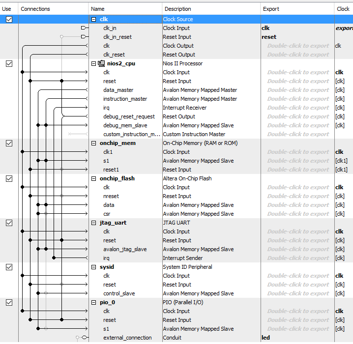 Note: The debug_reset_request signal from Nios® II processor must be connected to Nios® II reset signal.
Before you generate the Platform Designer (Standard) system, you may have some warning and error messages. This is due to the overlap of base address, reset vector and exception vector in Nios II processor which are not set to any memory devices.
- Double click on Nios® II Processor IP component to edit its parameters.
- Under the Vector tab:
- Select onchip_flash.data for Reset Vector to set the reset vector to On-chip Flash IP core.
- Select onchip_flash.data for Exception Vector to set the exception vector to On-chip Flash IP core.
- Under the JTAG Debug tab:
- Select Include JTAG Debug and set the number of hardware breakpoint to 4.
- Under the System tab, click on Assign Base Addresses.
- Following the steps 4-7 clears all warning and error messages. Click File>Save to save changes.
- Click Generate HDL... to generate the Platform Designer (Standard) system.