Visible to Intel only — GUID: iga1447091165720
Ixiasoft
Visible to Intel only — GUID: iga1447091165720
Ixiasoft
3.1.2. Connecting Signals to your Platform Designer System
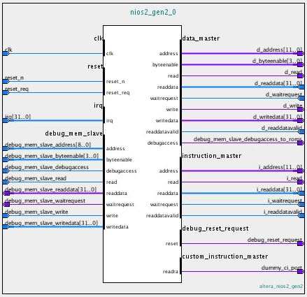
You must define the clock and reset pins for your Platform Designer system. You must also define each I/O signal that is required for proper system operation. The figure below shows the top-level block diagram of a Platform Designer system that includes a Nios® II processor. The large symbol in this top-level diagram, labeled std_1s40, represents the Platform Designer system. The flag-shaped pin symbols in this diagram represent off-chip (off-FPGA) connections.

For more information about connecting your FPGA design pins, refer to the Intel I/O Management, Board Development Support, and Signal Integrity Analysis Resource Center page of the Intel website.