Visible to Intel only — GUID: qzw1506028122456
Ixiasoft
Product Discontinuance Notification
1. Introduction
2. First Time Designer's Guide
3. Hardware System Design with Intel® Quartus® Prime and Platform Designer
4. Software System Design with a Nios® II Processor
5. Nios® II Configuration and Booting Solutions
6. Nios® II Debug, Verification, and Simulation
7. Optimizing Nios® II Based Systems and Software
3.1. FPGA Hardware Design
3.2. System Design with Platform Designer
3.3. Interfacing an External Processor to an Intel FPGA
3.4. Avalon-MM Byte Ordering
3.5. Memory System Design
3.6. Nios® II Hardware Development Tutorial
3.7. Platform Designer System Design Tutorial
3.8. Hardware System Design with Intel® Quartus® Prime and Platform Designer Revision History
3.6.4.1. Analyzing System Requirements
3.6.4.2. Defining and Generating the System in Platform Designer
3.6.4.3. Integrating the Platform Designer System into the Intel® Quartus® Prime Project
3.6.4.4. Developing Software with the Nios® II Software Build Tools for Eclipse
3.6.4.5. Running and Debugging Software on the Target Board
3.6.4.6. Varying the Development Flow
3.6.5.1. Install the Design Files
3.6.5.2. Analyze System Requirements
3.6.5.3. Start the Intel® Quartus® Prime Software and Open the Example Project
3.6.5.4. Create a New Platform Designer System
3.6.5.5. Define the System in Platform Designer
3.6.5.6. Integrate the Platform Designer System into the Intel® Quartus® Prime Project
3.6.5.7. Download the Hardware Design to the Target FPGA
3.6.5.8. Develop Software Using the Nios® II SBT for Eclipse
3.6.5.9. Run the Program on Target Hardware
3.6.5.5.1. Specify Target FPGA and Clock Settings
3.6.5.5.2. Add the On-Chip Memory
3.6.5.5.3. Add the Nios® II Processor Core
3.6.5.5.4. Add the JTAG UART
3.6.5.5.5. Add the Interval Timer
3.6.5.5.6. Add the System ID Peripheral
3.6.5.5.7. Add the PIO
3.6.5.5.8. Specify Base Addresses and Interrupt Request Priorities
3.6.5.5.9. Generate the Platform Designer System
3.7.1. Software and Hardware Requirements
3.7.2. Download and Install the Tutorial Design Files
3.7.3. Open the Tutorial Project
3.7.4. Creating Platform Designer Systems
3.7.5. Assemble a Hierarchical System
3.7.6. Viewing the Memory Tester System in Platform Designer
3.7.7. Compiling and Downloading Software to a Development Board
3.7.8. Debugging Your Design
3.7.9. Verifying Hardware in System Console
3.7.10. Simulating Custom Components
3.7.11. View a Diagram of the Completed System
3.7.4.1.1. Create a New Platform Designer System and Set up the Clock Source
3.7.4.1.2. Add a Pipeline Bridge
3.7.4.1.3. Add a Custom Pattern Generator
3.7.4.1.4. Add a PRBS Pattern Generator
3.7.4.1.5. Add a Two-to-One Streaming Multiplexer
3.7.4.1.6. Verify the Memory Address Map
3.7.4.1.7. Connect the Reset Signals
3.7.4.1.8. Save the System
3.7.4.2.1. Create a New Platform Designer System and Set Up the Clock Source
3.7.4.2.2. Add a Pipeline Bridge
3.7.4.2.3. Add a Custom Pattern Checker
3.7.4.2.4. Add the PRBS Pattern Checker
3.7.4.2.5. Add a One-to-Two Streaming Demultiplexer
3.7.4.2.6. Verify the Memory Address Map
3.7.4.2.7. Connect the Reset Signals
3.7.4.2.8. Save the System
4.1.1. Intel Command-Line Tools for Board Bringup and Diagnostics
4.1.2. Intel Command-Line Tools for Flash Programming
4.1.3. Intel Command-Line Tools for Software Development and Debug
4.1.4. Intel Command-Line Nios® II Software Build Tools
4.1.5. Rebuilding Software from the Command Line
4.1.6. GNU Command-Line Tools
4.1.6.1. nios2-elf-addr2line
4.1.6.2. nios2-elf-gdb
4.1.6.3. nios2-elf-readelf
4.1.6.4. nios2-elf-ar
4.1.6.5. Linker
4.1.6.6. nios2-elf-size
4.1.6.7. nios2-elf-strings
4.1.6.8. nios2-elf-strip
4.1.6.9. nios2-elf-gdbtui
4.1.6.10. nios2-elf-gprof
4.1.6.11. nios2-elf-gcc and g++
4.1.6.12. nios2-elf-c++filt
4.1.6.13. nios2-elf-nm
4.1.6.14. nios2-elf-objcopy
4.1.6.15. nios2-elf-objdump
4.1.6.16. nios2-elf-ranlib
4.2.2.4.1. Software Example Designs
4.2.2.4.2. Selecting the Operating System (HAL versus MicroC/OS-II RTOS)
4.2.2.4.3. Configuring the BSP Project
4.2.2.4.4. Configuring the Application Project
4.2.2.4.5. Makefiles and the Nios® II Software Build Tools for Eclipse
4.2.2.4.6. Building and Running the Software in Nios® II Software Build Tools for Eclipse
4.4.4.1. Performance Counter Advantages
4.4.4.2. Timer Advantages
4.4.4.3. Performance Counter and Timer Hardware Considerations
4.4.4.4. Performance Counter and Timer Software Considerations
4.4.4.5. Performance Counter Software Considerations
4.4.4.6. The Global Counter
4.4.4.7. Hardware Considerations
4.4.4.8. Tutorial: Using Performance Counters and Timers
4.4.5.1. nios2-elf-gprof –annotated-source Switch Has No Effect
4.4.5.2. Writing to the Registers of a Nonexistent Section Counter
4.4.5.3. Output From a printf() or perf_print_formatted_output() Call Near the End
4.4.5.4. Fitting a Performance Counter in a Hardware Design That Consumes Most
4.4.5.5. The Histogram for the gmon.out File Is Missing, Even Though My main()
5.2.1. Introduction to Nios® II Booting Methods
5.2.2. Nios® II Processor Booting from On-Chip Flash (UFM)
5.2.3. Nios® II Processor Booting from EPCQ Flash
5.2.4. Nios® II Processor Booting from QSPI Flash
5.2.5. Nios® II Processor Booting from On-Chip Memory (OCRAM)
5.2.6. Nios® II Processor Booting from CFI Flash
5.2.7. Summary of Nios® II Processor Vector Configurations and BSP Settings
5.2.3.1. Intel FPGA Serial Flash Controller (EPCQ) Overview
5.2.3.2. Nios® II Processor Design, Configuration, and Boot Flow
5.2.3.3. Nios® II Processor Application Execute-In-Place from EPCQ Flash
5.2.3.4. Nios® II Processor Application Copied from EPCQ Flash to RAM Using Boot Copier
5.2.3.5. EPCQ HAL Driver
5.2.4.1. Nios® II Processor Design, Configuration and Boot Flow
5.2.4.2. Nios® II Processor Application Executes In-Place from General Purpose QSPI Flash ( Intel® MAX® 10)
5.2.4.3. Nios® II Processor Application Copied from General Purpose QSPI Flash to RAM Using Boot Copier ( Intel® MAX® 10)
5.2.4.4. Nios® II Processor Application Executes In-Place from Configuration QSPI Flash (Other FPGA devices)
5.2.4.5. Nios® II Processor Application Copied from Configuration QSPI Flash to RAM Using Boot Copier (Other FPGA devices)
5.3.1. Assumptions About the Reader
5.3.2. Implementing a Custom Boot Copier
5.3.3. Default Nios® II Boot Copier
5.3.4. Advanced Boot Copier Example
5.3.5. Implementing the Advanced Boot Copier Example
5.3.6. Small Boot Copier Example
5.3.7. Implementing the Small Boot Copier Example
5.3.8. Debugging Boot Copiers
5.3.9. Externally Controlling the Nios® II Boot Process
5.3.5.1. Setting Up the Software Tools and Development Board
5.3.5.2. Creating a Suitable Hardware Design
5.3.5.3. Building the Advanced Boot Copier
5.3.5.4. Building a Test Application to Boot
5.3.5.5. Packing the Test Application in a Boot Record
5.3.5.6. Booting Directly From CFI Flash Memory
5.3.5.7. Booting CFI or EPCS/EPCQ Flash From On-Chip Memory
5.3.5.8. Running the Advanced Boot Copier Example
6.2.1.1.1. Nios® II System ID
6.2.1.1.2. Project Templates
6.2.1.1.3. Configuration Options
6.2.1.1.4. Nios® II GDB Console and GDB Commands
6.2.1.1.5. Nios® II Console View and stdio Library Functions
6.2.1.1.6. Importing Projects Created Using the Nios® II Software Build Tools
6.2.1.1.7. Selecting a Processor Instance in a Multiple Processor Design
7.4.1. Downloading the Ethernet Acceleration Design Example
7.4.2. The Structure of Networking Applications
7.4.3. The User Application
7.4.4. Structure of the NicheStack Networking Stack
7.4.5. Ethernet Device
7.4.6. Benchmarking Setup, Results, and Analysis
7.4.7. Nios® II Test Hardware and Test Results
7.5.1. Reasons for Using Tightly Coupled Memory
7.5.2. Tradeoffs
7.5.3. Guidelines for Using Tightly Coupled Memory
7.5.4. Tightly Coupled Memory Interface
7.5.5. Building a Nios® II System with Tightly Coupled Memory
7.5.6. Generate the Platform Designer System
7.5.7. Run the Tightly Coupled Memories Examples from the Nios® II Command
7.5.8. Program and Run the Tightly Coupled Memory Project
7.5.9. Understanding the Tcl Scripts
Visible to Intel only — GUID: qzw1506028122456
Ixiasoft
5.2.6.2.15.2.6.3.1. Hardware Design5.2.6.2.15.2.6.3.1. Hardware Design
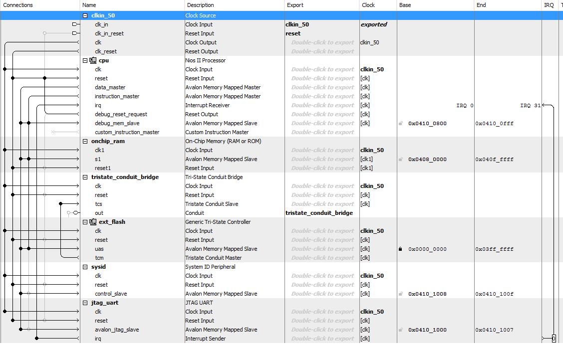
- Create your Intel® Quartus® Prime project and Platform Designer design.
- Make sure OCRAM or External RAM is added into your Platform Designer system.
- Refer to diagram below for example IP connections in Platform Designer.
Figure 179. Figure 204. Example IP Connections in Platform Designer for Booting Nios II from CFI Flash
IP Component Settings
- In the Nios® II processor parameter editor, set the Reset vector memory to CFI flash and Exception vector memory to OCRAM / External RAM or CFI flash according to your design preference.
Note: Setting the exception vector memory to OCRAM / External RAM is recommended to make the interrupt processing faster.
- If exception vector memory is set to CFI Flash, the minimum exception vector offset that you can set is 0x20.
Note: When executing-in-place, the Nios® II processor boots and runs directly from CFI flash, without copying any code at boot time. Because the Nios® II begins executing at the reset address in this case, exception vectors must be located at a nonzero exception vector offset to allow for 32 bytes instructions between the reset vector and the base of the exception vectors.
- The Reset vector must be the base address of your application. In this example, it is 0x01bc0000.
Note: Your *.sof image size influences your reset vector offset configuration. The reset vector offset is the start address of the .hex file in CFI flash and it must point to a location after the *.sof image. You can determine the minimum reset vector offset by using the following equation:
minimum reset vector offset = (.sof image start address + .sof image size) in HEX
Figure 180. Figure 205. Nios® II Parameter Editor Settings with Exception Vector Set to OCRAM / External RAM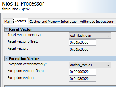 Figure 181. Figure 206. Nios® II Parameter Editor Settings with Exception Vector Set to CFI Flash
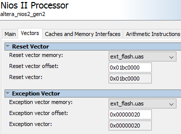
- If exception vector memory is set to CFI Flash, the minimum exception vector offset that you can set is 0x20.
- In Generic Tri-State Controller IP parameter editor, select one of the preset configurations in Library to automatically assign the parameter values.
Figure 182. Figure 207. Generic Tri-State Controller Preset ConfigurationIf your flash device is not listed in the Library, you can use the parameter editor to specify the required settings.
 Note: The appropriate values for these parameters are typically listed in the device’s datasheet.On top of the device specific parameters, ensure the following settings are correct in place:
- In Signal Selection tab, enable the following signals:
- readdata
- writedata
- read
- write
- chipselect
- address
Figure 183. Figure 208. Signal Selection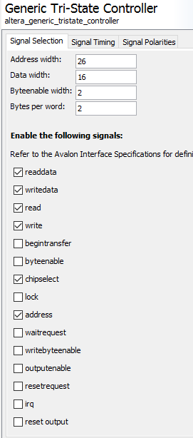
- In Signal Polarities tab, enable the following signals:
- read
- write
- chipselect
Figure 184. Figure 209. Signal Polarities
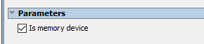
- In Parameters tab, select Is memory device.
Figure 185. Figure 210. Parameters Window
- In Avalon® Connection Point Assignments tab, set the following parameters to a value of 1:
- embeddedsw.configuration.isFlash
- embeddedsw.configuration.isMemoryDevice
- embeddedsw.configuration.isNonVolatileStorage
Figure 186. Figure 211. Avalon® Connection Point Assignments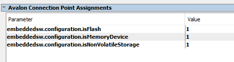
- In Signal Selection tab, enable the following signals:
- Click Generate HDL. The Generation dialog box appears.
- Specify output file generation options, and then click Generate.
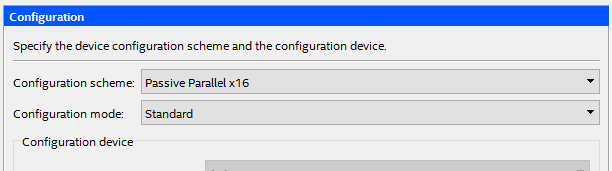
Intel Quartus Prime Software Settings
- In the Intel® Quartus® Prime software, click on Assignments > Device > Device and Pin Options > Configuration. Set Configuration scheme to Passive Parallel x8/x16/x32 1821
Figure 187. Figure 212. Configuration Scheme Selection
- Click OK to exit the Device and Pins Options window.
- Click OK to exit the Device window.
- Click on Processing > Start Compilation to compile your project and generate the .sof file.
1821 Set data width according to supported scheme.